This is a page describing my PDP-11 implementation done in a Xilinx xc6slx16 and written in Verilog
Sometimes 2011.
I decided 10 years ago that I needed to renew my engineering skills, and started to read about hardware design languages.
My first attempt to actually write something produced some flashing led's, and I proceeded to get TG68 running (a 68000 implementation)on a Spartan 3 kit, which took me a week or so, with the result of being able to execute a small hack that echoed characters.
Unfortunately, bad things happened in my family life that made me shelf the project until later.
July 2019
Unpacking a moving box, I found the Spartan 3 kit, and begun to restore the development system and see if I could get it to work again.
I had lost all software, but could download the Xilinx ISE, and after searching the internet found a helpful soul, Salvador E. Tropea who provided me with the linux based programming utility to get the code into the Spartan 3. (Thanks Salvador!). I was now able to write small Verilog or VHDL snippets and test them out. Now, what should I do with this thing? After some thinking, I decided to attempt to build a PDP-11, since that was the second computer I worked with back in 1974, and I felt that my half-century old knowledge of it's quirks and merits would be helpful in determining my skills in Verilog and FPGA design. It is very useful to have a "Golden Reference".So, I searched the Internet and found various implementations of PDP-11 in a FPGA. I selected Brad Parkers (Thanks Brad!) implementation since it was written in Verilog, that I felt had most similarity to the "C" language that I had done som hacking in in my previous life.
This is what a REAL PDP-11/70 looks like (the CPU box).
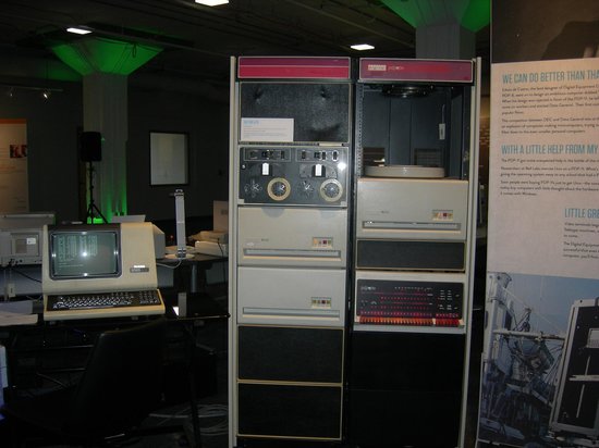
This is almost what I have implemented.The disk drives here are RL01/RL02 where mine are 8 emulated RK05 on a laptop PATA disk, and I do not have any tape emulation.
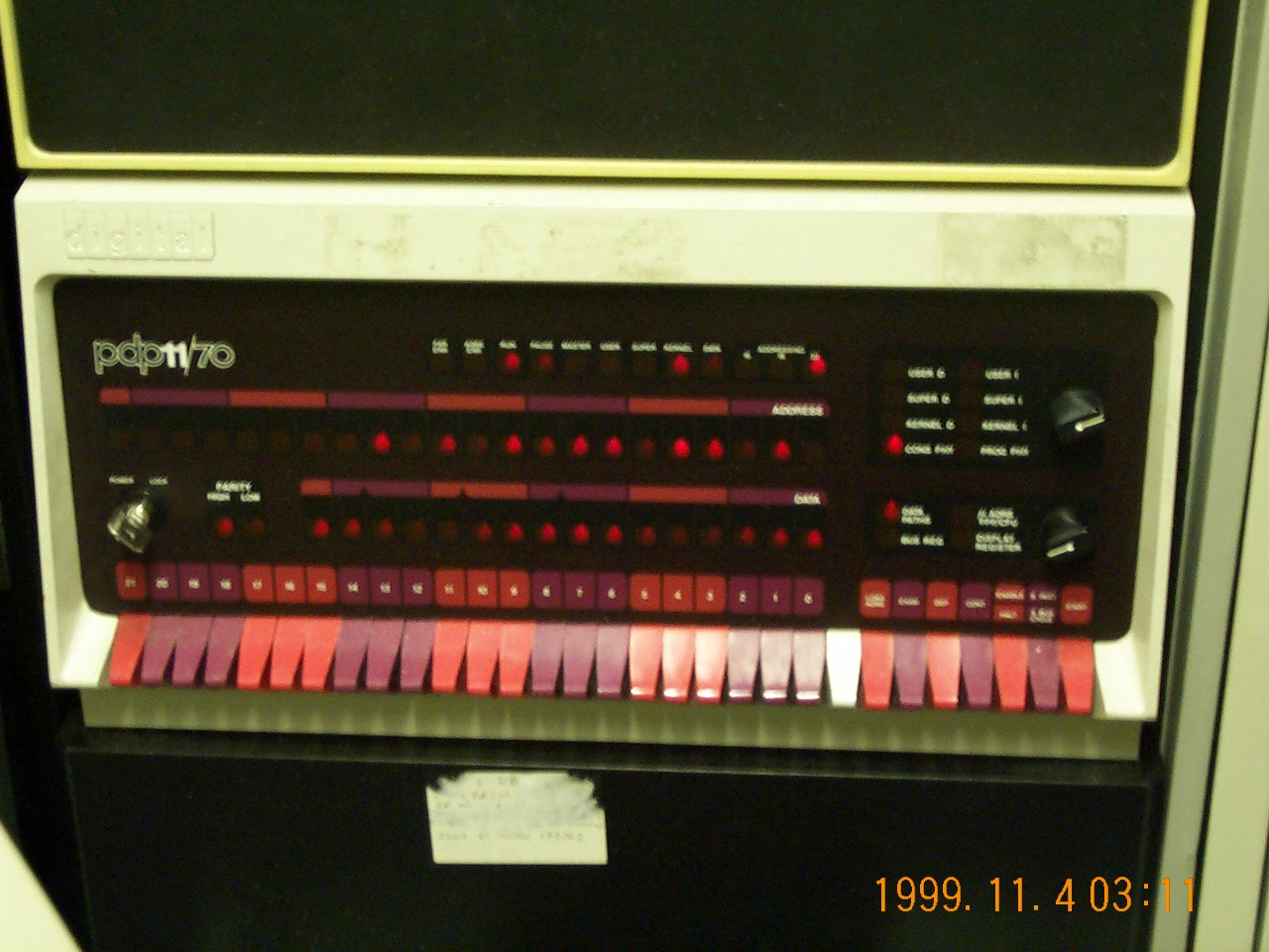
And this is what a PDP-11/666 can look like.
July-2020.
A year later. The PDP-11/666 now boots and runs RT-11, and currently outperforms a PDP-11/70 by a factor of 4.5 running the PI benchmark with 3000 decimals.
This beeing a Hobby project, with learning as main driving force, I have spent most of my time aligning the Verilog source, and making sure ALL PDP-11 diagnostics pass, except for a few exceptions of cosmetic nature. There are also some "future features" that are not yet implemented.
The PDP-11/666 runs on the Avnet Spartan 3 development kit, as well as on a QMTECH Spartan 6 board. The Spartan 6 board has 32 Mb of ram, which is not yet used, and breaks compatibility with the Avnet kit, so both have ram implemented within the FPGA. The QMTECH Spartan 6 board is also available with 256 Mb ram, so maybe that would be a candidate for a future VAX in a FPGA.
Ok, I could not resist, so I just ordered 2 of these.
Nov-2020.
New QMTECH boards have arrived, but I am still working on the old ones. I am currently debugging memory management, that has many interactions with a base PDP-11. I am very close to having it working, memory mapping works fine, I can set up PARs and PDRs to map memory, and execute code there or access data, but XXDP will not boot the XM monitor, and some diagnostics still fail. MTPD/MTPI/MFPD/MFPI works ok, but there is still some detail missing.
When I get through this, I will attempt to boot RSX-11M or maybe BSD, and also implement my own SDRAM code which will bring me up to 4 Mb of memory. Once all this works, I will probably attempt a FPGA VAX, just for the heck of it. This will be a "new" project, since my understanding of the VAX is much more limited than the old PDP, but I feel instruction fetching/decoding etc. is so similar, that the main focus should be on the memory management bits, and this will be written in conjunct with a console debugger/monitor. This will allow a more rapid development cycle as compared with what I have today.
Feb-2021.
Now I have spent some evenings, transforming the mmgt code, running mmgt test programs, and today the PDP-11/666 passes the PDP-11/24 memory management diagnostics. Proof of the pudding is below, booting up RT11 show the cpu as PDP-11/34, and also recognizes 64KB of memory ( as opposed to 56 KB) and also sees the memory mgmt hardware.
PDP 11/34 Processor
64KB of memory
Extended Instruction Set (EIS)
Memory Management Unit
50 Hertz System Clock
Extended unit support
Device Status CSR Vector(s)
------ ------ --- ---------
RK Resident 177400 220
DL Installed 174400 160
DU Not installed 172150 154
DD Installed 176500 300 304
TT (Resident)
RK (Resident)
RK0 = DK , SY
MQ (Resident)
DL
DD
TT (Resident)
3 free slots
.
Now, if I just had 4 Mb of memory, which incidentely is already ON the Fpga board, in the form of a 32 Mb SDRAM. But, there is no controller for it.....
It seems there is no SDRAM controller as IP in ISE 14.7, som I might have to do it from scratch.
Sometime-2021.
So, I just HAD to write my own SDRAM controller.
4 Mb of memory on line. I can run RT-11 test programs, reading and writing all memory. I can even copy
a snippet of code to the various pages of memory, end execute it
However, I still cannot boot XXDP-XM, and since I have no sources it is hard to debug the boot procedure.
August-2021.
The whole shabang seems to be working except for the fact that I cannot do DMA to the SDRAM. SDRAM differs from
LOW RAM by two things. LOW RAM is implemented with FPGA BlockRam and is located 0 - 64 kb. SDRAM is run by my
SDRAM controller, which currently takes 70 nS to do a read or write, due to the states of RAS. CAS, read access etc.
It is located at adresses 64k up to 4Mb. I left the old ram in to have "working" memory when doing test programs.
The controller signals completion of operation with a "ready" flag, and this works properly on CPU acesses.
However, it does not seem to work properly on DMA accesses. I have written a small DMA controller that can read or write
a single word on any DMA address by writing the address into a couple of registers in I/O space and setting a r or w bit
This should do a single DMA cycle to any location in memory, and is just a debug tool.
September-2021.
Simulation shows that I can in fact read a word using the DMA debug controller. Next is writing a word, and then implementing
this into the FPGA. Using ODT which is built in, I can deposit / examine both directly and via DMA hopefully